Navigazione principale
Navigazione principale
PhD Top Stories
Sara Fiori
Toxic gas detected and trapped by a carbon network: a new generation of devices?
Doctoral Programme in Nanotechnology
One of the major challenges of our generation in the near future is to paint our world and life-style with a green color. The use of renewable energy and the human impact on the environment are attracting increasing interest in the scientific community. Such an extraordinary challenge requires the use of a new generation of materials, among which the so-called two-dimensional (2D) materials play a pivotal role. This new 2D world opened up a fascinating playground of scientific wonders and practical applications, generating excitement in several fields and in particular in the nanotechnology community, the scientific branch involving science, engineering and technology in the study of materials at the nanoscale (as atoms). A nanometer is a billionth of a meter and, on such scale, materials often exhibit an unexpected behavior that attracts the scientist�s curiosity. The most widely known 2D material is graphene (Gr), firstly isolated in 2004 from graphite (the material pencils are made of). In Gr, carbon (C) atoms are arranged in a honeycomb structure and connected by strong covalent bonds. It is this particular structure that confers Gr its extraordinary properties, which can be tuned to widen its application fields. One approach for modifying specific Gr properties is the substitution of some C atoms in the network with different elements like, for example, nitrogen (N). This �doping� procedure allows successfully tailoring Gr features, turning it, for example, into a sensing material or allowing the activation of specific catalytic processes, like the oxygen reduction reaction. However, obtaining N-doped Gr (N-Gr) is not trivial and the production of high-quality layers is sometimes troublesome and tedious. In order to address this issue, we developed a new growth protocol for an easy and reproducible production of N-Gr on nickel (Ni), based on the well-known chemical vapor deposition approach. This technique exploits the catalytic activity of a metal substrate, in our case Ni, which, exposed to hydrocarbon molecules, �breaks� their chemical intra-bonds and allows for the rearrangement on the surface of C atoms, forming the typical Gr structure. We combined this procedure with the possibility to �push-down� (into the Ni bulk) and �pop up� (at the Ni surface) N atoms under specific conditions. During Gr growth, N emerging from the Ni bulk remains embedded in the mesh, creating N doping centers in the network (Fig.1).

Figure 1: Sketch of (a) Ni doping process with N (b) subsequent exposure to ethylene (c) formation of N-Gr.
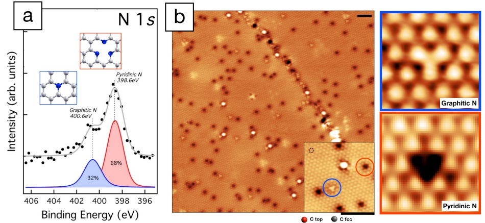
We studied the resulting N-Gr layer by experimental techniques such as scanning tunneling microscopy (STM) and X-ray photoemission spectroscopy (XPS). We revealed the presence of two different N configurations in the Gr mesh (Fig.2a), involving a variable number of N atoms: (i) �graphitic�, 1N, and (ii) pyridinic, 3N. By STM, a particular microscope which allows imaging single atoms on a surface, we �directly� observed the N-Gr surface, which appears flat and sprinkled by features (Fig.2b), not present in pristine Gr, that we ascribed to N atoms in the two chemical species (i) and (ii) (Fig.2). Then, in order to study the reactivity towards gases, pristine and N-Gr were exposed to near-ambient pressure of carbon monoxide (CO), a dangerous and potentially lethal gas. Comparing the experimental results obtained for the two systems, we demonstrated that in both cases CO was trapped in the confined zone between Gr and the Ni substrate, where it is stably stored at room temperature and released after annealing at around 80�C. CO trapping is facilitated in case of N-Gr, which results more efficient to this purpose than the pristine layer. In conclusion, our new growth protocol produces N-Gr layers on Ni of high-morphological quality, capable to significantly react towards low CO concentrations, trapping it in the nanospace. These results can open the way to interesting developments for gas sensor and storage, with promising technological applications and implications in our daily life.

Figure 2: (a) N1s XPS spectrum (b) STM image showing several defects on the surface. In the inset, in red and blue circles, two of the most abundant types of defects, magnified in the right panels. Black scale bars correspond to a distance of only 2 nm.
Authors and affiliations
Sara Fiori1,2, Daniele Perilli3, Mirco Panighel2, Cinzia Cepek2, Aldo Ugolotti3, Alessandro Sala1,2, Hongsheng Liu3, Maria Peressi11, Giovanni Comelli1,2, Cristiana Di Valentin3, Cristina Africh22CNR-IOM, Laboratorio TASC,Trieste, Italy
3Dipartimento di Scienza Dei Materiali, Universit� di Milano-Bicocca, Milano, Italy
Contact
Sara Fiori, email: sara.fiori@phd.units.itReference
Sara Fiori, Daniele Perilli, Mirco Panighel, Cinzia Cepek, Aldo Ugolotti, Alessandro Sala, Hongsheng Liu, Giovanni Comelli, Cristiana Di Valentin, Cristina Africh�Inside-out� growth method for high-quality nitrogen-doped graphene
Carbon 171, 704 (2021)
DOI: 10.1016/j
Reference
Daniele Perilli, Sara Fiori, Mirco Panighel, Hongsheng Liu, Cinzia Cepek, Maria Peressi, Giovanni Comelli, Cristina Africh, Cristiana Di ValentinMechanism of CO Intercalation through the Graphene/Ni(111) Interface and Effect of Doping
Journal of Physisical Chemistry Letters 11, 8887 (2020)
DOI: 0c02447
Informazioni aggiornate al: 16.12.2020 alle ore 14:17
Contact: Webmaster - Università di Trieste pagina curata da: Research Doctorate


